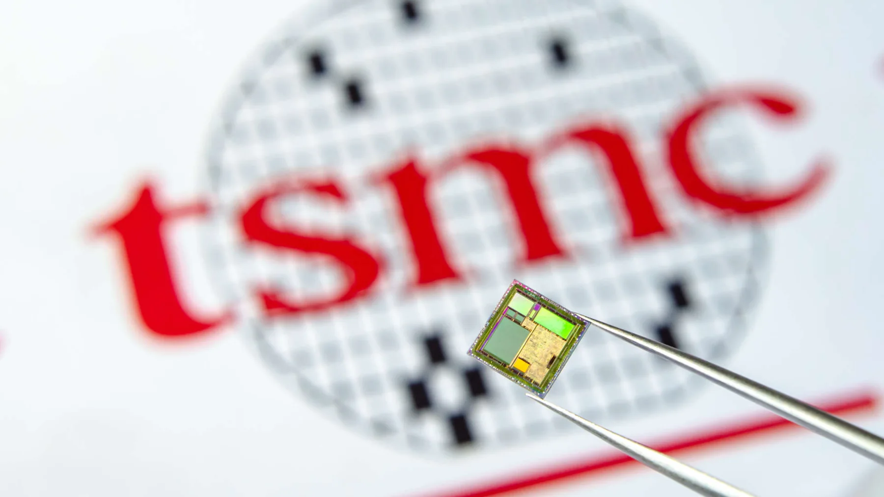
The semiconductor design automation space witnessed a historic achievement this week as electronic design automation (EDA) software giant Synopsys and foundry behemoth Taiwan Semiconductor Manufacturing Co. (TSMC) announced a significant expansion of their R&D collaboration.
The partnership will now include TSMC’s upcoming A14 (1.4nm) process node in its certified design enablement portfolio and formally introduce agentic AI into the EDA toolchain for digital, analog and multi-die packaging design flows.
1. Entering the A14 Era: Certified Flows for 1.4nm Silicon Design
As the foundry industry enters the sub-1.4nm era, traditional manual layout techniques will reach their physical limits. The newly established partnership enables certified design methodology from pre-silicon implementation through physical signoff on TSMC’s A14 process node.
Advanced Analog Routing Enablement: In analog design flows, where automated routing has traditionally been a challenge, Synopsys and TSMC have enabled full device routing on A14. This opens the door to automated analog place-and-route methodologies.
Analog Migration Automation: Using Synopsys Custom Compiler, designers can now migrate their existing analog layouts to the new process node with minimal manual intervention.
LLM-Accelerated Digital Implementation: With Synopsys Fusion Compiler, large language model (LLM) enhanced reasoning is applied to accelerate floorplanning and achieve faster-than-ever placement and routing convergence on billions of transistors.
2. Autonomous Chiplet Floorplanning with Agentic AI
As the physics limits of silicon-based semiconductors begin to take hold, HPC and AI processor developers are looking to heterogeneous integration of multi-die systems to bring performance improvements. Synopsys and TSMC have developed an autonomous agentic AI flow for chiplet floorplanning using the Synopsys 3DIC Compiler.
Automated Agent-Based Spatial Reasoning: A team of AI agents reason about spatial and interconnect constraints to develop multi-die layouts that maximize yield and performance. The new flow is qualified on TSMC’s 3DFabric ecosystem of advanced packaging technologies.
IVR Co-Design and Simulation: For next-generation AI accelerators and HPC processors, integrated voltage regulators (IVRs) are being pushed to new levels of performance. The new flow includes co-design and simulation of IVRs on TSMC CoWoS (Chip-on-Wafer-on-Substrate) interposer technology within a unified power integrity analysis environment.
CPO Design for Next-Generation Exascale Computing: Synopsys’ 3DIC Compiler now offers a unified CPO (Co-Packaged Optic) design environment targeting TSMC COUPE technology to address bandwidth limitations in modern data centers.
3. The Business Model Disruption: Subscription + Consumption for AI Agent Workflows
While most industry observers focused on the technical achievement of this R&D partnership, Synopsys is quietly disrupting the industry standard business model for EDA software.
The Rise of the Agentic Engineering Assistant: Rather than simply using AI to enhance existing EDA tools, the Synopsys R&D team has developed a suite of specialized AI agents that can perform complete design automation tasks as an autonomous engineering assistant.
Subscription and Consumption Licensing: As AI agent-based design automation replaces traditional human deskilled EDA tooling, Synopsys is moving away from conventional per-seat software subscriptions toward a consumption-based pricing model that reflects the underlying cloud compute costs.
4. Time to Enter the Physical AI Era
Synopsys’ collaboration with TSMC enables the semiconductor design automation industry to enter the physical AI era. By applying agentic AI to computationally intensive physical design tasks, EDA software vendors can now reduce design risk and time-to-market for advanced-node silicon projects.
Sources
- Sohail, O. (2025, August 28). Precision tweezers holding a semiconductor silicon die in front of a blurred TSMC background [Photograph]. Wccftech. https://wccftech.com/tsmc-breaking-ground-on-1-4nm-facility-initial-investment-of-49-billion/