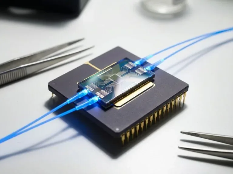
With tens of thousands of interconnected GPUs forming a single AI cluster, traditional copper interconnects are proving to be a significant power and thermal barrier as the bandwidth needs grow exponentially.
To meet this challenge posed by AI scaling, the semiconductor and optical networking industries are accelerating deployment of Co-Packaged Optics (CPO) and Silicon Photonics to push translation between electrical and optical signaling onto the same chip substrate as the compute silicon.
1. Breaking the Copper Limit: Why Pluggables are Hitting a Wall
For decades, data center networking has used pluggable optical transceivers that attach to the front panel of switches. But as switch bandwidths pass 51.2 Tbps and head for 102.4 Tbps while GPU interconnect needs double, traditional copper traces face insurmountable physics hurdles:
Reach & Loss: High-frequency electrical signals suffer insertion loss over copper traces on the printed circuit board (PCB).
Power Penalty: Pluggable transceivers require power-hungry digital signal processors (DSPs) and retimers to push signals over the PCB via electrical traces.
Thermal & Density Constraints: Sticking dozens of high-watt pluggable modules onto the face of a switch can cause unbearable heat density and restrict airflow.
2. Co-Packaged Optics (CPO): Moving Optics to the Silicon Substrate
Co-Packaged Optics (CPO) is eliminating these copper challenges by mounting photonic optical engines directly onto the same advanced packaging substrate as the switch Application-Specific Integrated Circuit (ASIC) or AI accelerator (XPU).
Eliminating the need for a long electrical pathway between the switch logic and photonic optical engine cuts the signal loss between them to the point where it eliminates the need to waste energy and space with high-power digital signal processor (DSP) retimers. The mass power reductions are allowing CPOs to reduce optical interconnect energy use to as little as 3.2 picojoules per bit.
It also creates room on the switch faceplate for ultra-high-density fiber array units (FAUs) to connect into the front panel directly. These benefits stem from the elimination of pluggable cages from the front of the switch.
3. Commercial Ramps: Foundries and Industry Heavyweights Lead the Charge
The push towards CPOs is going from a demonstration platform in the lab to commercial, volume production deployments with the arrival of key foundry capabilities:
TSMC COUPE Platform: TSMC’s new Compact Universal Photonic Engine (COUPE) technology utilizes 3D system-on-integrated-chips (SoIC) stacking to bond electrical die directly onto silicon photonic die, providing a key manufacturing foundation for future CPO products.
NVIDIA Spectrum-X Photonics: NVIDIA has partnered with TSMC to co-develop CPO switches that can utilize TSMC COUPE packaging to deliver ultra-high-density optical fabrics throughout large-scale AI/GPU clusters.
Broadcom Bailly CPO Platform: Broadcom is continuing to ramp their 51.2T and next-generation 102.4T CPO switch line cards, setting performance baselines for 100G/200G optical lanes and remote laser architectures.
External Light Sources (ELS): To address reliability concerns, many leading production CPO designs are isolating the heat-sensitive lasers in a field-replaceable Remote Laser Module (RLM) located away from the hot switch ASIC.
4. The Roadmap to Optical XPU Compute
While initial CPO volume is focused on scale-out networking switches, the endgame is scale-up optical I/O for XPUs with photonic optical engines placed directly on the GPU interposer along with High Bandwidth Memory (HBM).
As UCIe (Universal Chiplet Interconnect Express) standards evolve to support optical streaming modes, native optical chiplets will enable GPUs in different racks to communicate directly over light as if they were on a single local board.
Sources
- Laskey, R. (2026, February 13). An integrated photonic chip with connected fiber optic cables emitting blue light alongside tweezers [Photograph]. PhotonDelta. https://www.photondelta.com/blog/how-do-photonic-chips-compare-to-traditional-processors/