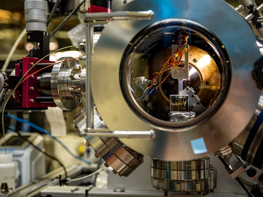
As the semiconductor industry moves towards high-numerical-aperture () Extreme Ultraviolet (EUV) lithography to print sub- logic nodes, traditional polymeric photoresists reach fundamental physical limits. Hyper-NA pitch scaling produces severe stochastic defects, line-edge roughness (LER), and photon shot noise due to ultra-thin resist film requirements ().
Researchers at Lawrence Berkeley National Laboratory (LBNL) and the U.S. Department of Energy (DOE) are utilizing specialized Photonic X-Ray Beamlines to study and characterize next-gen EUV photoresists. By using synchrotrons to create coherent soft X-ray and EUV radiation, these state-of-the-art beamlines provide sub-nanometer characterization, chemical reaction tracking, and extreme actinic exposure testing for future EUV photoresists.
1. Physical Bottlenecks in High-NA EUV Resist Physics
Transitioning from to EUV tool architectures severely shrinks optics depth-of-focus, forcing lithographers to utilize significantly thinner resist layers:
EUV Photon Shot Noise & Absorptivity Limits: EUV photons (, ) have high energy per photon, resulting in low total photon density per unit area. Low absorption probability in ultra-thin films causes severe statistical fluctuations (shot noise) during pattern transfer.
Secondary Electron Blur: Absorbed EUV photons cause low-energy secondary photoelectrons to be generated in the resist matrix. Random thermalization and isotropic scattering of secondary electrons broadens the effective exposure area, blurring printed line edges.
Stochastic Defects at Sub-2nm Features: Micro-bridging, nano-swelling, and line-break defects can occur when chemical secondary reactions do not reach completion in ultra-confined, high-aspect-ratio spatial regions.
2. Advanced Synchrotron Beamline Architecture & Actinic Metrology
DOE synchrotron facilities—such as the Advanced Light Source (ALS) at LBNL—feature beamlines specifically tailored for EUV photoresist metrology and characterization:
Coherent Soft X-Ray & Tunable EUV Photons: Synchrotron beamlines provide high-brightness spatially coherent light tunable over the soft X-ray and extreme ultraviolet spectrum (), enabling precise spectroscopic probing of core-level electron excitations.
Resonant Soft X-Ray Scattering (RSoXS): By tuning X-ray energy to absorption edges of specific elements (e.g., carbon, fluorine, tin, or iron), RSoXS can map spatial chemical heterogeneity, cross-linking density, and phase separation within resists at sub-nanometer resolution.
Actinic Interference Lithography (AIL): Beamlines split EUV beams to create ultra-high-density interference fringes, allowing researchers to evaluate resist resolution capabilities down to sub- half-pitches without utilizing costly High-NA scanner optics.
3. High-Absorption Material Architectures: Metal-Oxide Resists (MORs)
Using insights acquired from photonic beamline characterization, chemical material suppliers are shifting from traditional organic chemically amplified resists (CARs) to dense inorganic architectures:
Metal-Oxide Nanoclusters (SnOₓ / ZrOₓ / HfOₓ): Metal-oxide resists (MORs) utilize high- metals such as tin, zirconium, or hafnium. These elements have much higher absorption cross-sections at than organic carbon matrices, increasing energy gain in thin films.
Localized Secondary Electron Generation: Metal-oxide cores create short-range secondary electrons upon EUV absorption, limiting total electron blur radius and improving line-edge fidelity.
Etch Selectivity & Mechanical Stability: Inorganic MOR networks form extremely durable, dense cross-linked structures upon exposure which confer high plasma etch resistance during subsequent underlying silicon and dielectric etching steps.
4. In-Situ Chemical Dynamics & Yield Optimization Roadmaps
Beamline diagnostics allow researchers to observe physical and chemical phenomena in real time during actinic exposure:
Real-Time Outgassing & Degradation Analysis: Integrated mass spectrometry and photoemission spectroscopy on synchrotron beamlines measure volatile photo-products and outgassing species in situ, ensuring new MOR formulations do not contaminate scanner optics.
X-Ray Photoelectron Spectroscopy (XPS) Tracking: Time-resolved XPS tracks elemental state transformations, ligand loss, and metal-oxygen core condensation during and immediately after EUV exposure, finding reaction kinetics under operational vacuum conditions.
Accelerating Commercial Scanner Readiness: Fundamental reaction kinetics and physical data collected at LBNL/DOE facilities directly inform material synthesis at industrial photoresist manufacturers, reducing development cycles for High-NA and Hyper-NA () commercial fabrication processes.
Sources
- Lawrence Berkeley National Laboratory. (2026, August 24). Experimental vacuum chamber endstation at the Advanced Light Source (ALS) beamline [Photograph]. LBNL News Center. https://newscenter.lbl.gov/2026/08/24/planning-a-new-era-of-discovery-with-the-upgraded-advanced-light-source/